MIT engineers grow atomically thin transistors to make super dense computer chips
3 minute readPublished: Tuesday, May 2, 2023 at 8:02 am

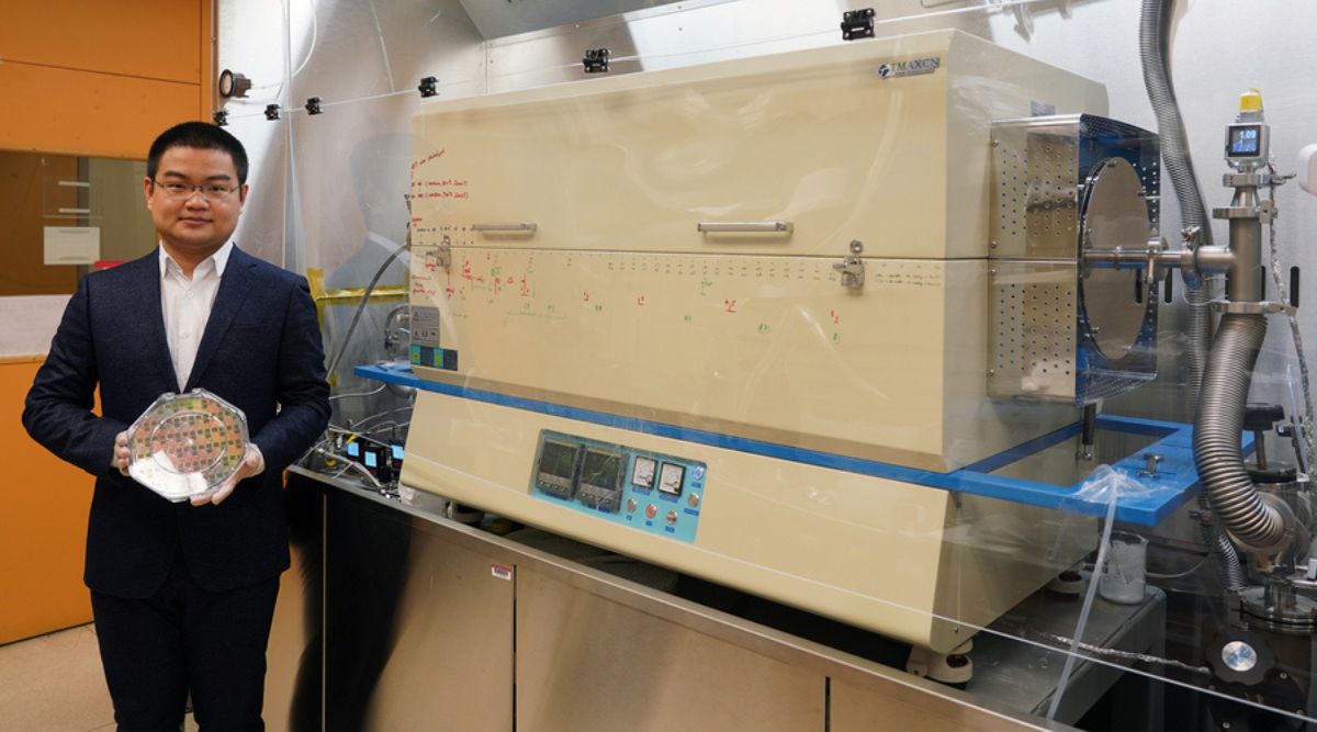
As humans have gotten more and more dependent on computers for life and work, the need for more powerful and denser computer chips has gotten greater. This is especially true with emerging AI applications including ChatGPT-like chatbots. Now, researchers at the Massachusetts Institute of Technology (MIT) have developed a new technology that could help us build much more denser circuits on computer chips. Conventionally, semiconductor chips like the one on the device you are using to read this are made using materials which have bulky 3D structures. Due to this, stacking multiple layers of transistors to make denser chips is quite difficult. This is where the researchers new method comes into play, according to MIT. In a study published in Nature Nanotechnology, the researchers document how they made semiconductor transistors using ultrathin 2D materials, each of which was about the thickness of three atoms. These transistors could be stacked up more densely to create more powerful chips. Growing transistors on a Silicon wafer With the new method, the engineers grew layers of 2D transition metal dichalcodenide materials on a fully fabricated silicon chip. In the past, researchers have tried growing 2D materials elsewhere and transferring them onto a chip or a wafer but this could cause imperfections that can impede the performance of devices. But at the same time, growing 2D materials directly onto a silicon wafer was challenging because the process typically requires temperatures above 600 degrees Celsius. This is a problem considering the fact that silicon transistors and circuits get damaged when heated to above 400 degrees. But the new technology consists of a relatively low-temperature growth process that does not damage the fully-fabricated chip. This tech can be used to directly integrate 2D semiconductor transistors on top of standard silicon circuits, according to MIT. This process can be used to grow a smooth, highly uniform layer across an 8-inch wafer, without the issues that come with growing the layer elsewhere and integrating it into the circuit. You can think about decomposition like making black pepper you have a whole peppercorn and you grind it into a powder form. So, we smash and grind the pepper in the high-temperature region, then the powder flows back into the low-temperature region, said Jiadi Zhu, co-author of the research article, in a press statement. Problems with the process Silicon circuits usually have aluminium or copper as a top layer so that the chips can be connected to a carrier before it is mounted on a circuit board. But the sulphur in diethylene sulphur, one of the organic molecules used in the process, sulphurises these metals. This is similar to how metals rust when they are exposed to oxygen, affecting their conductivity. To prevent this, the researchers first deposited a very thin layer of passivation material on top of the chip before putting it through the growing process. This passivation layer can then later be opened to make connections. Also, while the temperature is relatively lower compared to earlier methods, it still requires putting the chips in a furnace that operates at around 400 degrees Celsius. Because of this, they place the silicon wafer into a low-temperature region of the furnace vertically, rather than horizontally. By doing this, neither end of the chip is too close to the high-temperature region, so that no part is damaged by the heat. The future of the technology The researchers now plan to fine-tune their technique so that many stacked layers of 2D transistors can be grown in the future. Along with this, they also want to see how this low-temperature growth process can be adapted to flexible surfaces like polymers, textiles, or even papers. According to MIT, this could mean that semiconductors can be integrated into objects like clothing and notebooks.